Technology Summary
How to increase the packaging density of electronic product with integral substrate and advanced interconnect are prime issues needed to be addressed first in electronic packaging in order to meet consumers demand for light-weight, compact, reliable and multifunctional electronic or communication devices. In the aspect of high-density interconnection, nanoscale surface activated interconnect, nanowire/carbon-tube bump, etc. may dramatically increase the density of interconnection. In the aspect of integral substrate, built-in passive components with nanomaterials, such as resistors, capacitors, inductors and filters can remarkably increase the density of integral substrate. Therefore, nanomaterials applied for electronic packaging could be the solution to satisfy the needs for innovation and integration in information, communication and consumer electronics industries by enabling manufacturers to develop lighter, more compact, more integrated, and more competitive products.
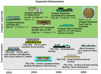
Current Status
Advanced interconnection:
Highly conductive polymer: studying the formation of high conductive polymer and its bumping.
Surface activated bonding technology: studying the activation mechanism both on metal and polymer surface.
Nanowire/carbon-tube bump technology: studying the vertical built-up and bonding mechanism of nanowire/carbon-tube.
Electrophoresis tiny chip assembly: studying the assembly process of ultra-small IC (< 200 µ m) with electrophoresis.
Integral substrate technology:
Design and Process technology: developing basic element electric models for embedded devices and the embedding process technologies, such as lamination and patterning, paste printing and ink-jetting.
Nanomaterials for embedded devices: developing organic/inorganic nanocomposite polymer for high-Dk/low-loss as well as ultra-low Dk substrate films, synthesis of materials with nanostructure for ultra-high Dk, precise resistance and inductance.
Accomplishments / Industry Impact
Integral Substrate: developing nanomaterials, to break through the bottleneck of functional materials currently applied in embedded capacitors, inductors and resistors; and to establish the infrastructure of advanced integral substrate through the development of design, processes technologies and the build-up of device model databank.
Advanced Interconnect: improving the drawbacks in current packaging processes, to develop super-conducting organic materials, and to accomplish next generation applied technologies for high-density, low-cost, and easy-to-rework, with fine pitch bumping and precision assembly.